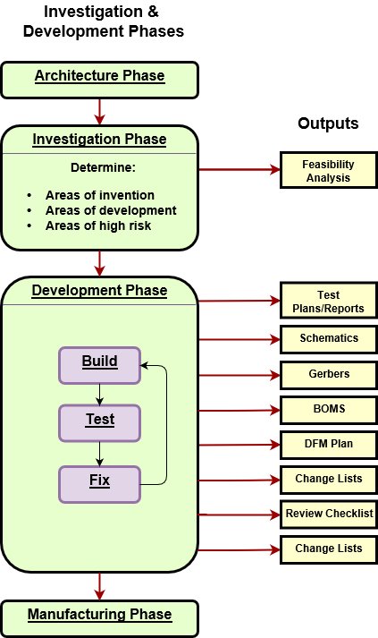
Once the architecture is established, you need to determine that the project is feasible. Is it doable given the leverage points available and the skillsets that can be applied? In order to determine this, identify major areas of risk, areas with no clear solution, and areas where new invention or new development is required. Then, create experiments and build prototypes to determine what is needed to address and prove out the areas of concern.
Investigation Phase – Key Information to Determine
- Areas of High Risk – Determine what areas may be very risky so that risk can be mitigated.
- Areas Requiring Invention – Figure out places where no existing solution will work and invention will be required. Relying on new invention is risky and may require an unknown amount of time to come to fruition.
- Areas Requiring Significant Deveopment – Figure out the areas that will require alot of engineering resources and multiple development cycles.
Once the experimentation has completed to investigate these areas of concern, a determination will be made about whether the project is feasible and should continue to the development phase.

The development phase is where the bulk of the work gets done for a project. Electrical engineers will be designing and building prototypes of the electronics, testing them, debugging issues, and implementing fixes for the next revision of prototype. This is commonly called the build-test-fix cycle that repeats until all major issues have been discovered and fixed, and the electronics are ready for prodction. In this discussion I will focuss on the development phase for a PCA or set of PCAs, because that is what I am familiar with. Other types of development like cables may be similar, but some other types like FPGA development are quite different from PCA development, since you are developing code rather than a physical object in that case.
Let’s start by talking about the EE prototype development process. This starts with the development of schematics where you implement the components for the PCA and connect them. While schematics are being developed, a Bill of Materials (BOM) is released so long leadtime components (components that take a long time to get) can be purchased ahead of the proto build. It is important to get a BOM out early, even if it may still need to change before the build, because often long leadtimes parts are the critical path to getting your protos built.
EE PCA Development Process
- Start Schematics
- Release Risk-Buy BOM ASAP – Get procurement going on long lead-time components
- Complete Schematics
- Host Design Review, Incorporate changes from review
- Setup Layout and place components
- Review with mechanical engineering
- Complete Layout and review with EEs
- Release Gerbers, BOM, and Schematics for fabrication
- Archive Design Files and documentation
Once schematics are complete, host a design review. As I have said before, I recommend splitting design reviews into to small, focussed meetings. Host a design review to cover functionality and firmware topics, host a review with operations to talk about supply chain and manufacturing and schedule, host a review with the EE team focussed on EE topics. Keep good notes from the design review; consider asking a colleague to keep notes for you during the meeting, so you can focus on the discussion. You will probably get alot of feedback during the reviews, some good feedback, some trivial or disagreable. It is helpful during the meetings to just take in the feedback and record it, and don’t try to decide on each item then and there, unless you think the topic of feedback could benefit from group discussion. In your own time, you can go through the feedback one by one. Address each item, do not accept some items and state the reasons why, implement the changes you think are good, and discuss items you are not sure about with colleagues. Then, send a message to all involved with the design review stating the result for each item of feedback.
Next: Manufacturing Phase
