Let’s try an example and go through the process of designing a simple state machine. Say we want to design a device that is called an Up/Down Counter. This device outputs a binary count, and it has two inputs: UP/DOWN_L, and RESET_L. Reset is active-low and when it is asserted (0) it overrides all and resets the count to 0. If RESET_L is not asserted (1) the counter counts up if UP/DOWN_L is high (1) and counts down if UP/DOWN_L is low (0). The plan is to make a two-bit version of the Up/Down counter with synchronous reset.
2-Bit Up/Down Counter With Reset
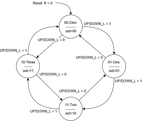
A 2-bit counter has four possible values: 00,01,10,11 (0,1,2,3 in decimal). So, we are going to need four states, and that means 2 D-FFs. Now, we will draw what’s called a Bubble Diagram that describes our state machine. Here are the steps to create a Bubble Diagram for our state machine.
- Draw a bubble (circle) for each State
- Number the top of each bubble with a binary number and count in grey code (00,01,11,10).
- Provide a Name for each state after its number (Zero, One, Two, Three)
- Draw a line in each bubble, and write the output values below the line
- Reset overrides everything, and we place that outside the circles with an arrow point to the reset state (Zero).
- Then, for each state think about the transitions you want to other states. And, draw an arrow indicating each valid transition out of each state. If you want to stay in a state under certain input conditions, draw an arrow looping back to that state.
- At the base of each arrow, write the state machine input signal names and indicate the value of all inputs for that transition to occur. “Don’t care” logic value can be used if an input has no effect on that transition. Don’t include global overriding inputs like reset.
Output Decoder
Start the output decoder design by creating a truth table. Write the State values as inputs and put corresponding outputs as indicated in the diagram above.
Output Decoder Truth Table
| STATE[1] | STATE[0] | OUT[1] | OUT[0] |
| 0 | 0 | 0 | 0 |
| 0 | 1 | 0 | 1 |
| 1 | 1 | 1 | 0 |
| 1 | 0 | 1 | 1 |
From the truth table, we need to write the Boolean Logic Equations for the two outputs. For each output, look at where it has a value of 1, then write the logic of the inputs that makes it 1.
OUT[1] = (STATE[1] • STATE[0]) + (STATE[1] • STATE[0])
Using the distributive property, we can rearrange to:
OUT[1] = STATE[1] • (STATE[0] + STATE[0])
Using the Law of Boolean Algebra, A + !A = 1, we can reduce to:
OUT[1] = STATE[1] • 1 = STATE[1]. So, the output decoder for OUT[1] is just a wire from STATE[1], which will be the Q1 FF1 output. Now, we need to do the same for OUT[0].
OUT[0] = (STATE[1] • STATE[0]) + (STATE[1] • STATE[0]); I don’t think this can be reduced.
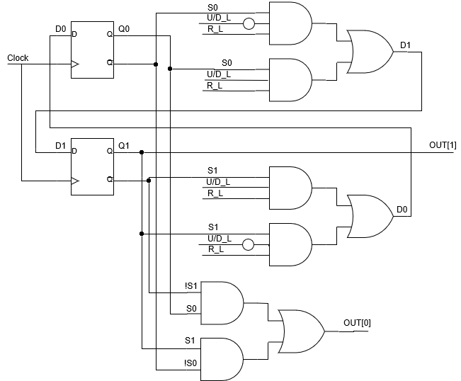
Output Decoder Schematic

Often in logic diagrams circles are used to represent inverters as with the two inputs to the AND gates above. This makes the diagrams more compact without having to draw the full inverter symbol.
Next State Decoder (NSD)
Using the Bubble Diagram we can construct a truth table for the next state decoder. The inputs for the next state decoder are the state signals (FF Q outputs) and other state machine inputs, which are UP/DOWN_L and RESET_L in this example. The outputs of the NSD are the “next state”…the D inputs to the FFs.
Start with Reset input. We always want the next state to be 00 when reset is low, so write D1,D0 = 0,0 on the lines where R_L = 0. Then look at each state in the bubble diagram and see what the next state is for each input combination. So, state Zero (00) will transition to state One (01) if UP/DOWN_L = 1, or it will transition to state Three (10) if UP/DOWN_L = 0. Continue for each state until the truth table is filled out.
| S1 | S0 | U/D_L | R_L | D1 | D0 |
| 0 | 0 | 0 | 0 | 0 | 0 |
| 0 | 0 | 0 | 1 | 1 | 0 |
| 0 | 0 | 1 | 0 | 0 | 0 |
| 0 | 0 | 1 | 1 | 0 | 1 |
| 0 | 1 | 0 | 0 | 0 | 0 |
| 0 | 1 | 0 | 1 | 0 | 0 |
| 0 | 1 | 1 | 0 | 0 | 0 |
| 0 | 1 | 1 | 1 | 1 | 1 |
| 1 | 0 | 0 | 0 | 0 | 0 |
| 1 | 0 | 0 | 1 | 1 | 1 |
| 1 | 0 | 1 | 0 | 0 | 0 |
| 1 | 0 | 1 | 1 | 0 | 0 |
| 1 | 1 | 0 | 0 | 0 | 0 |
| 1 | 1 | 0 | 1 | 0 | 1 |
| 1 | 1 | 1 | 0 | 0 | 0 |
| 1 | 1 | 1 | 1 | 1 | 0 |
That’s a pretty big truth table, isn’t it? I don’t know about you, but I don’t feel like writing out those long equations and reducing them. So, we will use a shortcut. There are lots of wonderful, specialized calculators out there on the internet, so let’s use one that reduces logic for us automatically. Note that in bygone days before computers, we would use a process called Karnaugh Maps, which is a pretty nifty way to simplify logic, but let’s just use the calculator. Here is one very helpful tool: http://www.32×8.com/. It takes in the truth table and provides simplified logic equations, and circuit drawings.


Complete State Machine
We have designed the output decoder and the next state decoder, so now we can hook up the whole state machine. The FFs used below have !Q outputs as well as Q, and I used them. Also, the circles indicate inverters. We did it! We completed a design of an Up/Down Binary counter with Synchronous Reset. This schematic can be implemented with components and wired up.