Different digital signalling technologies have been developed for logic chips, and parts that adhere to a particular signalling technology making them compatible are called a logic family. There are many logic families, but most are variations of TTL, CMOS, or LVDS. Each logic family provides chips with a variety of logic functions such as logic gates, buffers, flip-flops, and counters.
All logic families have key specifications that their parts abide to.
Basic Specifications
- Vcc or Vdd – Power Supply Voltage
- VIH – Minimum input voltage for valid logic high
- VIL – Maximum input voltage for valid logic low
- VOH – Minimum output voltage for logic high
- VIH – Maximum output voltage for logic low
- IOH – High-level output current
- IOL – Low-level output current
- Icc or Idd – Power supply current
- VI – Maximum input voltage to avoid damage
- tP – Various propagation delay specifications (from each input to each output)
CMOS
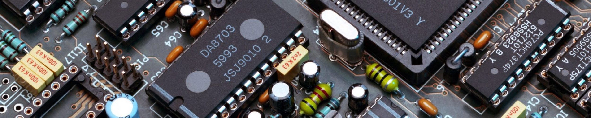
CMOS stands for Complementary Metal Oxide Semiconductor and is based on field effect transistors (FETs). Below is the circuit for a CMOS receiver and a driver. When implemented as an input the Vin node would be connected to an input pin and the Vout node would be connected to the interior circuitry of the chip, and when implemented as an output the Vout node would be connected to an output pin, and the Vin node would be connected to the interior circuitry of the chip.
CMOS Specs
You should always check the datasheet, but below are typical specifications for CMOS parts. Note that VIH and VIL are percentages of Vcc, which is quite different from the relation in TTL.
- VIH = .7 * Vcc
- VIL = .3 * Vcc
- Vcc = 1.8V, 2.5V, 3.3V, 5V
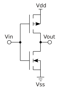
TTL
TTL stands for Transistor-Transistor Logic and is based on bipolar junction transistors.
TTL Specs
Read the datasheets, but in general TTL valid logic levels are below.
- VIH = 2.0V
- VIL = .8V
- Vcc = 3.3V, 5V
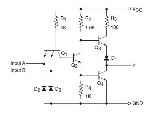
LVDS
LVDS stands for Low-Voltage Differential Signalling. It is differential signalling where two lines carry the signal, and the receiver uses the difference between the two input voltages, Vin+ minus Vin-. Differential signalling has a number of advantages over single-ended signalling. The lines can be routed close to each other which provides immunity to EMI. And, the driver drives the – half as the symmetric inverse of the + half, so the magnetic fields of the two signals cancel, which reduces the EMI that signal produces. Because of LVDS’s great immunity to noise, it can be driven with low voltage swings, which means it can be lower power than other I/O solutions. Low voltage swings also means that it can be driven faster and has more frequency bandwidth.
Advantages of Differential Signalling
- EMI Immunity
- Produces less EMI
- Low Voltage Swings
- Low Power
- High-Frequency Bandwidth
Here is a thorough guide on logic families from Texas Instruments: http://www.ti.com/lit/sg/sdyu001ab/sdyu001ab.pdf