
Characteristic Impedance
Electromagnetic waves do not propagate instantaneously. They propagate at the speed of light (3 x 10⁸ m/s) along a lossless conductor surrounded by vacuum, and at a slower speed when surrounded by material. As an electromagnetic signal propagates along a conductor, the ratio of its voltage amplitude to its current amplitude is called Characteristic Impedance, which has units of Ohms and we denote with the symbol Z0. Characteristic Impedance is not really the same thing as Impedance, which is a ratio of voltage across component(s) to the current through it(them). It is a characteristic of transmission lines experienced by propagating electromagnetic waves.
Characteristic Impedance is also the input impedance for a uniform transmission line of infinite length.

- j is the imaginary number
- R0 is characteristic resistance (Ω/m)
- G0 is characteristic conductance (Ω m)-1
- L0 is characteristic inductance (Henrys/m)
- C0 is characteristic capaictance (Farads/m)
- ω is natural frequency (radians/s)
For real-world conductors, it is a good assumption to neglect resistance and conductance, which greatly simplifies characteristic impedance. This assumption is called a lossless transmission line.

Transmission Line Model
Lossy Transmission Line
Lossless (Ideal) Transmission Line
Propagation Delay
Signal propagation delay, which is the inverse of propagation speed, is the square root of characteristic inductance times characteristic impedance. And, it is also equal to the square root of the dielectric constant of the material surrounding the conductor divided by the speed of light.


- L0 is characteristic inductance
- C0 is characteristic capacitance
- εr is dielectric constant of surrounding material
- c is speed of light (3 x 10⁸ m/s)
- tPD has units of time/distance
It is rather a surprising result that propagation delay depends only on εr. And it is because changes in conductor geometry that affect C0 have an exactly compensating effect on L0.
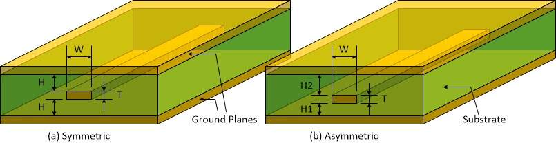
Propagation in PCBs
Printed circuit boards are usually made up of multiple conductive layers. Conductors on inner layers (stripline) are completely surrounded by PCB insulating material, and conductors on outer layers (microstrip) have PCB insulating material beneath them and air above. This mixed environment for outer conductors causes their propagation delay to be dependent on an effective dielectric constant, which is a combination of that of the PCB material and that of air. Dielectric constant for air is about the same as that for vacuum, which is 1.
εr of Vacuum = 1; εr of Air ≈ 1
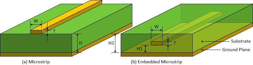
Effective Dielectric Constant for Outer Conductors

Inner layers (Stripline): 
Outer layers (Microstrip): 
Standard PCB material is FR4, which has a dielectric constant around 4.0 and effective dielectric for outer layers of 2.92. With these values:
Inner Layers: 
Outer Layers: 
Lumped Element vs Distributed Element Systems
When do you need to worry that signals take time to propagate? The answer for analog signals is when the wavelength of a signal is approximately the same size or shorter than the length of the conductor. Wavelength is equal to the inverse of propagation delay times frequency in Hz.

When wavelength is long compared to conductor length, we consider the system a Lumped Element system and do not worry about transmission line effects. When signal wavelength is on the order of the conductor length, we need to worry about transmission line effects.
For digital signals it is the rise or fall time, which ever is faster, that is compared to the propagation time to determine whether the system can be treated as lumped parameter or as distributed. Here are some rules of thumb.
Rules of Thumb
Analog Signals: Critical conductor length is 1/4 the wavelength of highest frequency component. Conductors longer than this are transmission lines.
Digital Signals: Critical conductor length is 1/6 the physical length occupied by rising or falling edge, whichever is faster. Conductors longer than this are transmission lines.
Let’s do a digital example. You have a clock signal with rise and fall time equal to 1ns, and your FR4 PCB trace length from crystal oscillator to microcontroller is 3 inches long on an outer layer. Will this signal have transmission line effects?

Length of Rising Edge = 
The conductor length is 3 inches, which is more than 1/6 the length of the rising edge, so you need take steps to mitigate transmission line effects.
Reflections
If a transmission line has no change in characteristic impedance along its length, and if we assume the transmission line is lossless, then a voltage or current signal will be transmitted down the line without attenuation or distortion. If the transmission line is somewhat lossy, then the signal amplitude will be attenuated some. If the transmission line has changes in characteristic impedance down the line, then the signal will be distorted due to signal reflections that occur at each place where characteristic impedance changes.
When a propagating wave (incident wave) encounters a change in impedance, a wave will be reflected back towards the driver (reflected wave), and a wave will be transmitted beyond the impedance discontinuity (transmitted wave).
Reflected Wave Voltage: 
Transmitted Wave Voltage: 
Transmitted Wave Voltage = Incident Wave Voltage + Reflected Wave Voltage
- VI is the incident voltage wave
- VR is the reflected voltage wave
- Γ12 is the reflection coefficient
- Τ12 is the transmission coefficient
Reflection Coefficient:
Transmission Coefficient: 
Let me make some observations:
- The reflection coefficient can never be more than 1
- If Z02 is small compared to Z01, the reflection coefficient approaches -1
- If Z02 is big compared to Z01, the reflection coefficient approaches +1
- If Z02 is equal to Z01, the reflection coefficient is 0 – no reflection
- The transmission coefficient can never be more than 2.
- The real portion of the transmission coefficient will always be positive, because the real portion of characteristic impedance is always positive. So, the transmitted wave will not switch sign (+ or -).
Driver and Receiver
The origin of a signal propagating along a transmission line is called a driver or source. And, the destination of the signal is called a receiver or load. The circuitry of driver and receiver have impedances that are experienced by propagating signals and can cause reflections. Specifically, it is the Thevenin equivalent impedance of a driver and receiver that is used for reflection calculations.
For digital circuits driver output impedance is low (~20Ω – 50Ω) and receiver input impedance is high (~1MΩ). To determine the Thevenin equivalent resistance of the driver, select the nodes where the the source (voltage source VS and its output impedance RS) connect to the transmission line and set your point of view to look in to the source from the transmission line. Nullify VS by shorting it, and the Thevenin equivalent resistance is then RS.
The Thevenin equivalent impedance of the receiver is easy to determine…it is just RL.
Thevenin Eq Impedance of Driver = RS
Thevenin Eq Impedance of Receiver = RL
For a digital signal, let’s talk through what happens when the driver transitions the logic state of the signal, for example a low to high transition.
The Voltage source Vs drives the signal high, and the first thing the signal encounters is a voltage divider formed between the source resistance Rs and the characteristic impedance of the transmission line Z0. The voltage transition wave that actually flows down the transmission line is a divided down version of Vs: Vs * Z0 / (Rs + Z0). This wave travels down the uniform transmission line unperturbed until it reaches load RL. If RL is not equal to Z0, a reflection is generated. The receiver at the load would receive the transmitted wave, which is the incident wave plus the reflected wave, and the reflected wave would travel back towards the source.
Once the reflected wave reaches the source, if Rs is not equal to Z0, there is an impedance discontinuity and another reflection would be generated, travelling towards the load. Very messy.
The time it takes for the waves to bounce around and reach a steady-state value is called settling time. When settled, the final value at the load will be the value for a lumped parameter system without transmission line effects. In the circuit above it would be the voltage divider value VS * RL/(RL + RS), involving just the load and source resistances, not the characteristic impedance of the transmission line, because that is a transitory phenomenon.
Here is a nice visualization:
Next: Termination