
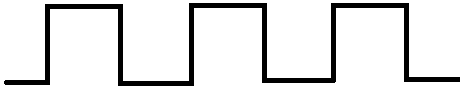
Synchronous logic refers logic that changes on a set cadence, logic changes at set intervals of time. A square wave signal called a clock signal is used to drive the synchronous changes in a logic circuit. Logic changes when the clock signal transitions from low to high (rising edge) or from high to low (falling edge). Computers, Smart Phones, and many other electronic devices are mainly gigantic synchronous logic circuits.
Logic Changes when Clock Transitions
RS-Latch
The most basic form of a synchronous logic circuit is the Set-Reset Latch. This device is created by cross-coupling two NAND gates. It is the feedback of the outputs connected to the inputs that turns the combinatorial NAND logic gates into a synchronous logic circuit.
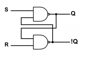
Truth Table – RS-Latch
| S | R | Q | !Q |
| 0 | 0 | latch | latch |
| 0 | 1 | 0 | 1 |
| 1 | 0 | 1 | 0 |
| 1 | 1 | 0 | 0 |
When R (reset) is high and S (set) is low, the output is “reset” to 0, and when S is high and R is low the output is “set” to 1. When both R and S are low, the output retains its previous value 0 or 1; this is called latching. The state where both S and R are high is considered an invalid state for this device. The outputs of the RS-Latch change when the reset or set input transitions logic states (after some propagation delay).
D-Latch
By adding on to the RS-Latch, we can avoid the invalid input state and modify the behavior to create the D-Latch.
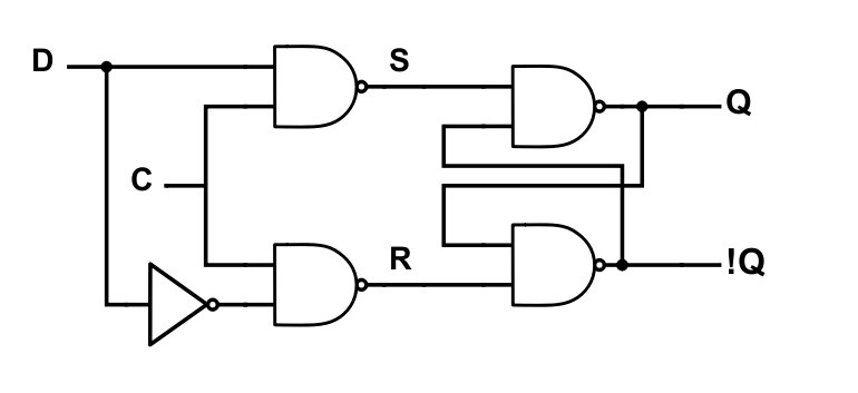
Truth Table – D-Latch
| C | D | Q | !Q |
| 0 | X | latch | latch |
| 1 | X | D | !D |
An “X” in a truth table means “don’t care” or “either value”. When C (clock) is high, output Q follows input D (data). When clock transitions low, output Q latches it current value and keeps that value until clock goes high again. Output !Q always has the inverse value of output Q. Sometimes the C input is called E meaning “enable”. Voilà the D-Latch.
D-Flip-Flop
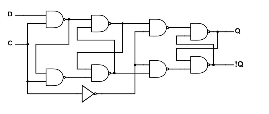
Truth Table – D-Flip-Flop
| D | C | Q | !Q |
| X | 0 | Q | !Q |
| 0 | ⭡ | 0 | 1 |
| 1 | ⭡ | 1 | 0 |
The D-Flip-Flop only changes its output on the rising edge of the clock input. On a rising edge of clock, the output Q is updated to reflect the value of input D (data) whether it be 0 or 1. When clock is not transitioning from low to high, Q retains the value it acquired at the last positive clock edge. Output !Q always just holds the inverse of output Q.
D-Flip-Flops are the basis for state machines and much of large scale synchronous logic circuits.
D-Flip-Flop With Set/Reset
D-Flip-Flops may additionally have set (S) and reset (R) inputs. These inputs may be synchronous, meaning the output Q gets set (1) or reset (0) on the clock edge, or asynchronous, meaning the output Q gets set or reset when the set or reset input is asserted.
Symbols


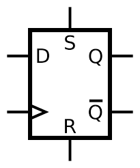
In D-Flip-Flip symbols the > character is often used to indicate the clock input. Q with a bar over it means Not Q or the inverse of Q.
There is another type of Flip-Flop called a JK-Flip-Flop. It has the same flippy-floppy behavior of latching a value on a signal edge, but is a bit different than D-Flip-Flops. Frankly, I don’t think it is important to learn that device, since modern electrical engineers only rarely implement discrete flip-flop and latch devices. Instead, we implement programmable logic devices, which we will discuss at some point, that have the capability of 1000’s even millions of D-Flip-Flops all in one chip. Or, we perform the required logic with software or firmware in a processor or microcontroller. Or, we implement specialized logic devices that contain flip-flops.
However, it is crucial to understand the concept of a flip-flop, the concept that when a clock edge occurs, data on the input is transferred to the output. And, when there is no clock edge, the device holds or stores the previously latched data value on its output.
Next: Logic Families